Table of Contents
- Introduction
- GPU Hardware Model
- SM — Streaming Multiprocessor
- CUDA Programming Model
- Thread Hierarchy in Practice
- The Matrix Multiplication Problem
- The Roofline Model
- Three CUDA Kernels
- Nsight Compute Results
- Conclusion
1. Introduction
Matrix multiplication is the backbone of AI. You can think of every operation, convolution, diffusion, attention, as a way to multiply matrices. Thankfully, matrix multiplication is embarrassingly parallel, which is great news for us. Companies realised this and started throwing GPUs at the problem. The rest is history!
This blog is my journey to understand both matrix multiplication and the hardware it runs on. Starting with attention in the last post brought me here. And understanding GPUs will help me get closer to the real question: how can we make AI inference faster?
This blog looks at both the hardware and software sides of GPUs. I have focused on NVIDIA GPUs and CUDA because most of the big LLM companies lean on NVIDIA hardware for inference and training. The goal is to slowly build one core understanding: how do I know if my model is performing well or badly? If I understand the machine, I understand its performance.
2. GPU Hardware Model
CPU vs GPU
The easiest comparison I always reach for is a Ferrari versus a School Bus. CPUs are Ferraris. GPUs are School Buses.
CPUs have a few high-performance cores that can execute one task extremely fast. GPUs have thousands of moderately performing cores, structured in a way that lets you run the same operation across all of them simultaneously. The Ferrari gets one person from A to B faster than anything else on the road. The School Bus carries 40 people from A to B at once. Cumulatively, the school bus has moved more mass in the same time.
That is the GPU in one analogy. Not faster at any single thing. Massively faster at doing the same thing many times over.
Matrix multiplication fits this perfectly. Each output element C[i][j] is an independent dot product. No element depends on any other. You can compute all of them simultaneously. Throw 1000 cores at 1000 independent dot products and you finish in the time it takes to compute one. That is why GPUs exist. That is why every major AI company runs their training and inference on NVIDIA hardware.
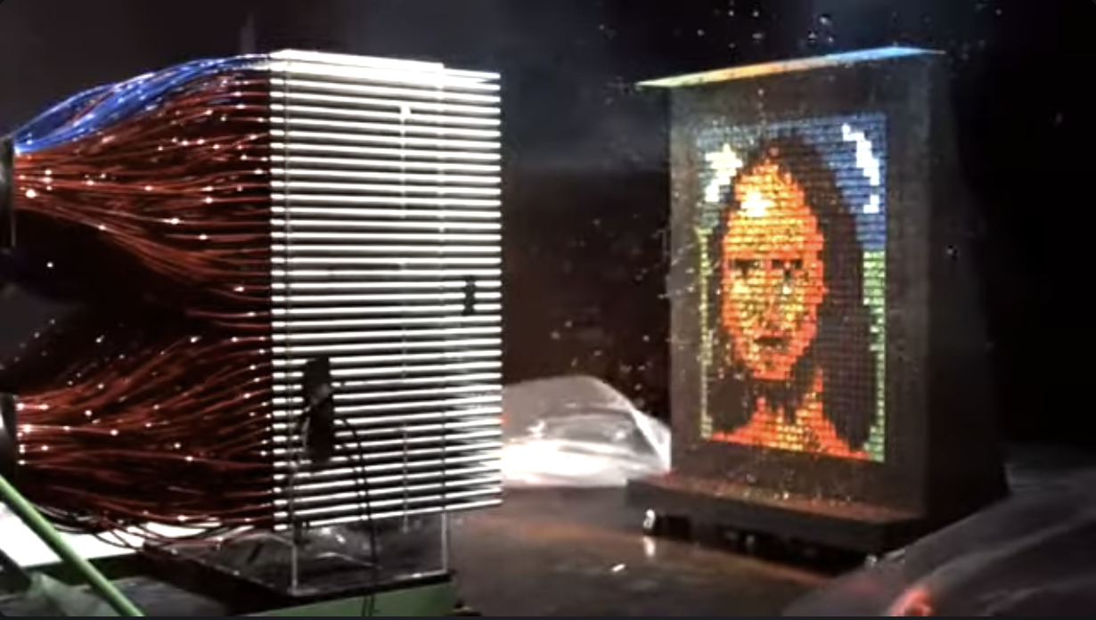
MythBusters + NVIDIA — painting the Mona Lisa one pixel at a time (CPU) vs all at once (GPU). Click to watch on YouTube.
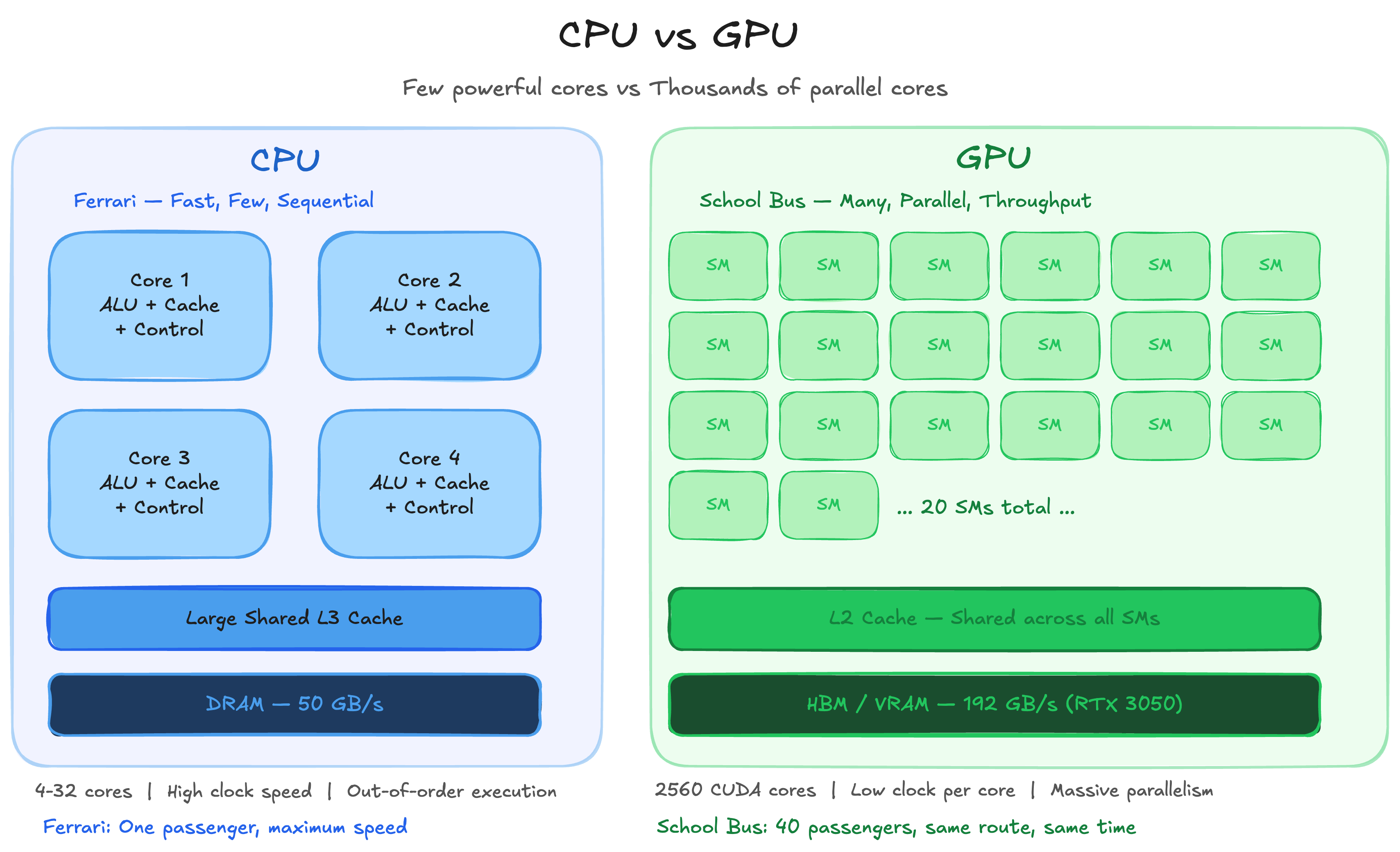
CPU vs GPU — Few powerful cores vs thousands of parallel cores
3. SM — Streaming Multiprocessor
The SM is the most fundamental unit on a GPU. It is very similar to what we know as a core in a CPU. Both execute computation and store state in registers, with associated caches.
Before arriving at the SM design, NVIDIA used to have specialised cores for specialised tasks like shaders, rasters and so on. This architecture was painful on both sides. Software engineers had to map programs onto a fixed pipeline. Hardware engineers had to guess the load ratios between pipeline steps. The SM design solved both problems by making every unit general purpose.
GPU SMs are simpler and weaker processors than CPU cores. Execution within an SM happens at the instruction level with no speculative execution or branch prediction.
A quick note on what those mean:
Speculative Execution: the CPU predicts what might happen next and starts executing instructions before it is certain they are needed. If the prediction was right, results are kept. If not, the CPU rolls back and executes the correct path.
Branch Prediction: decides whether a branch will be taken and what the target address will be. This feeds speculative execution with a direction to run in.
GPUs skip all of this. Simpler hardware, more of it.
Although GPU SMs are weaker than CPU cores individually, they execute far more threads in parallel. Throughout this blog we follow one fixed calculation: 1 Warp = 32 Threads. Each SM contains a Warp Scheduler, L0 instruction cache, Dispatch Unit, Register File, CUDA Cores and Tensor Cores.
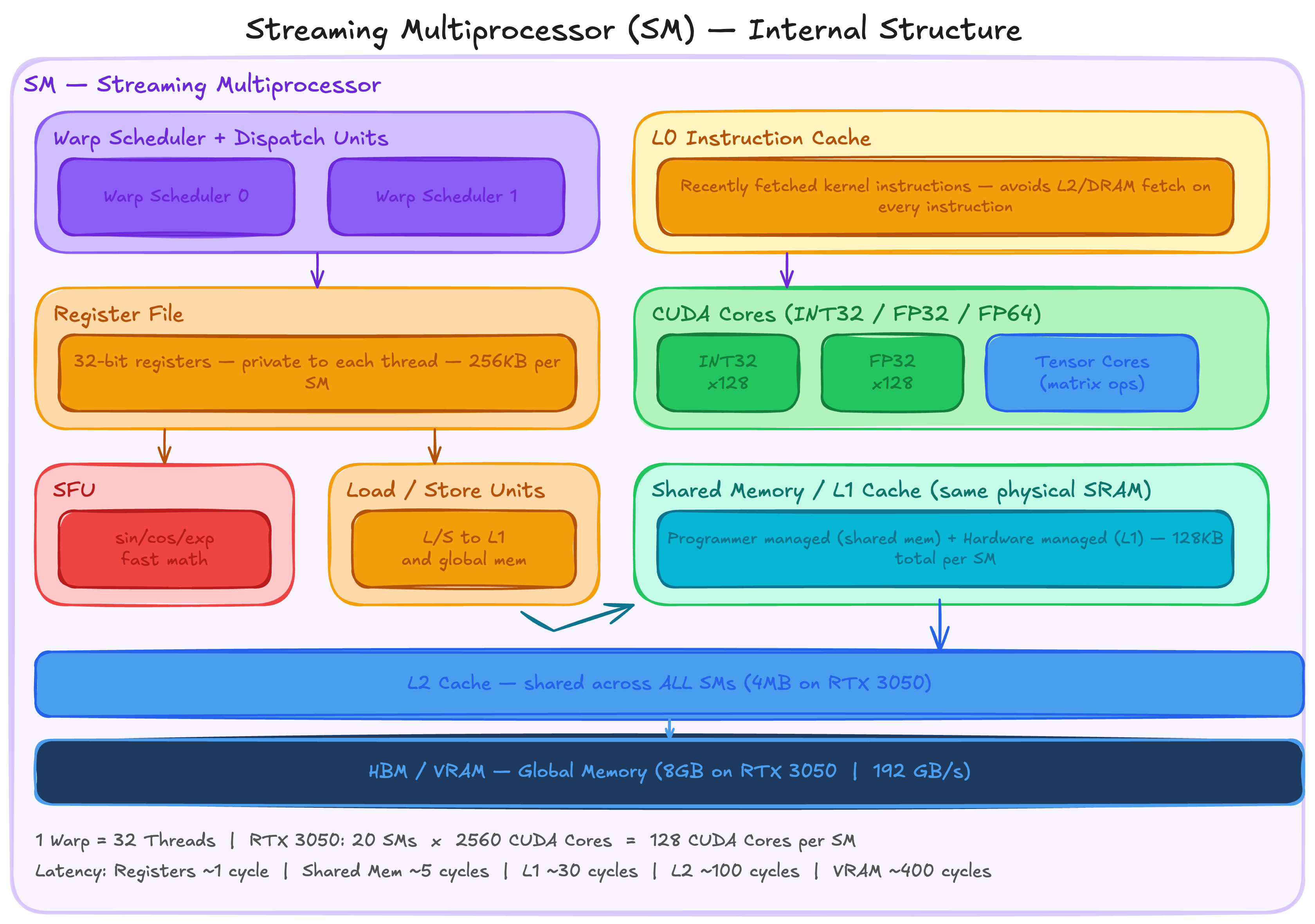
Streaming Multiprocessor (SM) — Internal Structure
GPU SMs support a large number of concurrent threads whose instructions are interleaved over time. Here is how that works in practice:
Warp A requests data from memory. This takes hundreds of clock cycles. Instead of waiting, the SM keeps Warp A in play and continues executing Warps B, C and D. The GPU keeps thousands of threads in play and rotates between them so it never sits idle.
The analogy I keep coming back to is a chef. He puts water to boil for Dish A. While it boils, instead of waiting, he chops vegetables for Dish B and prepares utensils for Dish C. The number of available tasks and the speed at which he can switch between them determines how well he hides latency. Delays from waiting for the water to boil, the pressure cooker to settle and so on. For the GPU, latency comes from memory reads, thread synchronisations and other expensive instructions. More warps in play means more opportunities to hide that latency and keep the CUDA and Tensor Cores fed with work.
SM Components in Detail
Special Function Units, Load/Store Units, Instruction Cache and Shared Memory
Special Function Units accelerate certain arithmetic operations within the SM. Mathematical operations like exponential, sin, cos and similar functions have dedicated hardware here rather than being computed through the general CUDA cores. Fast and cheap for the operations that need them.
Load/Store Units dispatch requests to load and store data to the memory subsystem of the GPU. They interact directly with L1 cache (SRAM) and indirectly with off-chip global memory. Indirect here means: if the data is not in cache, the cache controller fetches it from main memory and sends it to the processor. This is the path that causes the latency that the warp scheduler works so hard to hide.
Instruction Cache (L0 Cache) sits at the front end of an SM. Its job is to hold recently fetched kernel instructions so the warp scheduler does not have to go to L2 cache or DRAM every time it issues an instruction. When there is an instruction cache miss, the warp scheduler immediately switches to another eligible warp. If instruction cache occupancy is too low, the SM stalls completely.
Shared Memory is user managed cache. The typical programming pattern is to stage data coming from device memory into shared memory, process it there, and write the output back to device memory. This is exactly what tiled matmul does, which we will get into later in this post.
Warp Scheduler
The Warp Scheduler is the unit inside the SM that decides which group of threads to execute on each clock cycle. It also manages the execution state of all active warps.
Warps are switched out on a per clock basis, roughly every nanosecond. The scheduler rapidly switches between concurrent warps as soon as their instruction operands are available. This is exactly how GPUs hide latency. No warp sits idle waiting for memory if there is another warp ready to run. Each thread has its own private registers allocated from the register file of the SM.
L1 Cache
L1 caches in GPUs are entirely programmer managed, unlike CPUs where the hardware manages them. They are shared between the warps scheduled together. This design means context switches in GPUs have almost no impact on cache hit rates. There is very little data movement needed to save and restore state when switching between warps, which is a significant part of why GPU context switching is so fast compared to CPU context switching.
Register File
The register file of the SM is the primary store of bits between their manipulation by the CUDA and Tensor Cores. It is split into 32-bit registers that can be dynamically allocated between different data types. These physical registers back the virtual registers in the PTX intermediate representation. Allocation of physical registers to threads in SASS (Streaming Assembler) is managed by a compiler like ptxas.
One important implication: the number of registers a kernel uses directly affects how many warps can be active simultaneously on an SM. More registers per thread means fewer concurrent warps means less latency hiding. This is the register pressure tradeoff you will see in Nsight Compute output.
CUDA Cores and Tensor Cores
Although they are called cores, CUDA Cores and Tensor Cores are nothing like CPU cores. As we already saw, the SM is the closest equivalent to a CPU core. The term core here is used very loosely. It simply means a pipeline that takes an input, performs an operation, and returns an output.
CUDA Cores execute scalar arithmetic operations. Instructions issued to CUDA cores are not independent — they are issued as a group by the warp scheduler and applied to different registers simultaneously. That group size is 32, which is the warp. Depending on the SM architecture, CUDA cores can contain different units: INT32, FLOAT32 and FLOAT64.
Tensor Cores operate on entire matrices with a single instruction. Operating on multiple data points in one instruction fetch reduces power requirements dramatically compared to issuing individual scalar operations.
A concrete example: the HMMA16.16816.F32 SASS instruction calculates D = AB + C for matrices A, B, C and D where C and D are the same physical matrix. MMA stands for Matrix Multiply and Accumulate. The 16 refers to half precision input float. F32 is the single precision output float.
What is that number 16816? It encodes the matrix dimensions m, n, k as 16, 8, 16. Multiplying them out: 16 x 8 x 16 = 2048 MAC operations performed by a single instruction.
One important note: a single instruction in a single thread does not produce the entire matrix multiplication. The 32 threads of a warp cooperatively produce the result together. Most of the per-instruction power overhead is in decoding, which is shared across the warp by the warp scheduler. Even after spreading across 32 threads that is 2048 / 32 = 64 MAC operations per thread per instruction.
GPU RAM and HBM
GPU RAM uses Dynamic RAM (DRAM), which is dramatically slower than SRAM but much larger. It is usually not on the same die as the SMs. In the latest GPUs, DRAM is located on a shared interposer alongside the GPU die for decreased latency and increased bandwidth. This is what we now call HBM, High Bandwidth Memory.
How does bandwidth actually get calculated? The formula is straightforward:
Bandwidth = (Bus Width x Clock Rate) / 8Two examples to make this concrete:
RTX 3050 uses GDDR6. Bus width is 128 bits across 4 chips of 32 bits each. Effective clock rate is 14 Gbps. Bandwidth = (128 x 14) / 8 = 224 GB/s.
A100 uses HBM2e. Bus width is 5120 bits, dramatically wider than GDDR6. Effective clock rate is 2.4 Gbps, actually lower than GDDR6. Bandwidth = (5120 x 2.4) / 8 = 1,536 GB/s. That is roughly 7x higher than the RTX 3050 despite the lower clock rate. The width wins.
HBM does not win on clock speed. It wins on bus width. More lanes, more data per cycle, dramatically higher bandwidth. This is why A100s and H100s dominate inference workloads where memory bandwidth is the binding constraint.
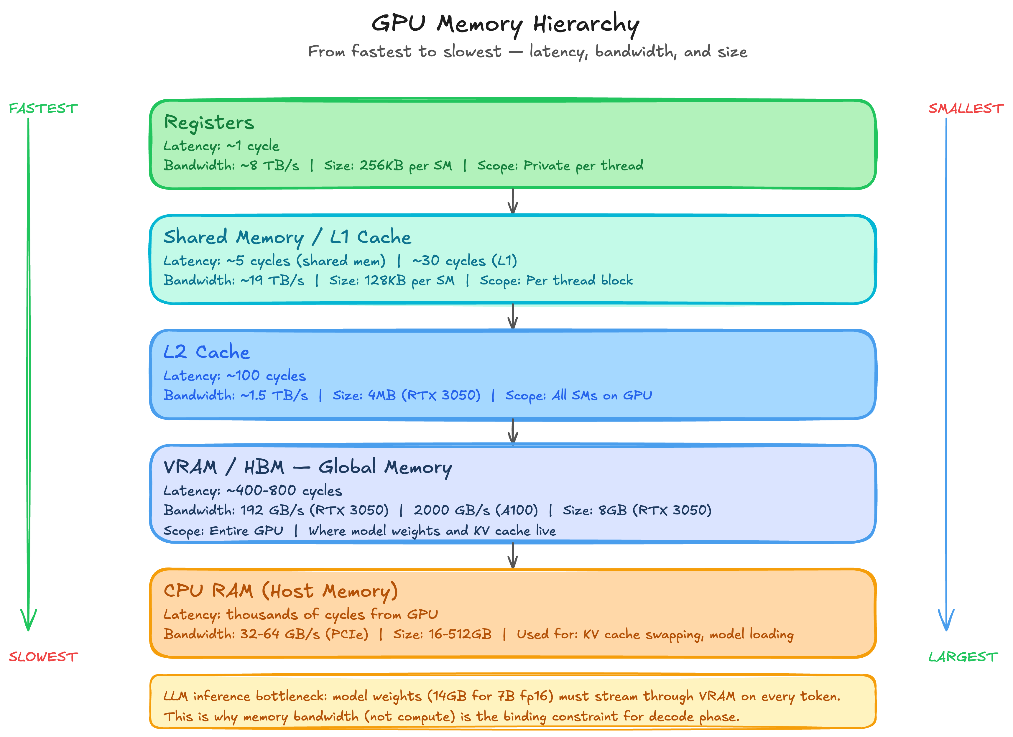
GPU Memory Hierarchy — from registers (~1 cycle) to HBM (~400 cycles)
4. CUDA Programming Model
In this section we map the GPU hardware architecture to the programming model. How do we translate all the hardware parts we discussed into software concepts? That is the question this section answers.
There are three major parts to the CUDA programming model.
1. Hierarchy of Threads
Programs are executed in threads. The CUDA Core and Tensor Core we discussed in the hardware section are essentially what we refer to as threads in the programming context. Programs can reference groups of threads in a nested hierarchy, from individual threads to blocks to grids.
2. Hierarchy of Memories
Thread groups at each level of the hierarchy have access to a corresponding memory resource. Accessing the lowest layer of the memory hierarchy is fast and as good as executing an instruction. As you move up the hierarchy the memory gets larger, slower and further from the compute.
3. Thread Synchronisation
Thread groups coordinate execution through barriers. Threads need to sync up with each other frequently to avoid one thread overwriting data that another thread is still using and to prevent race conditions entirely.
The programming model is implemented using two low-level formats: PTX (Parallel Thread Execution) which is both an instruction set architecture and an intermediate representation, and SASS (Streaming Assembler) which is the lowest-level human readable format output by the NVCC compiler.
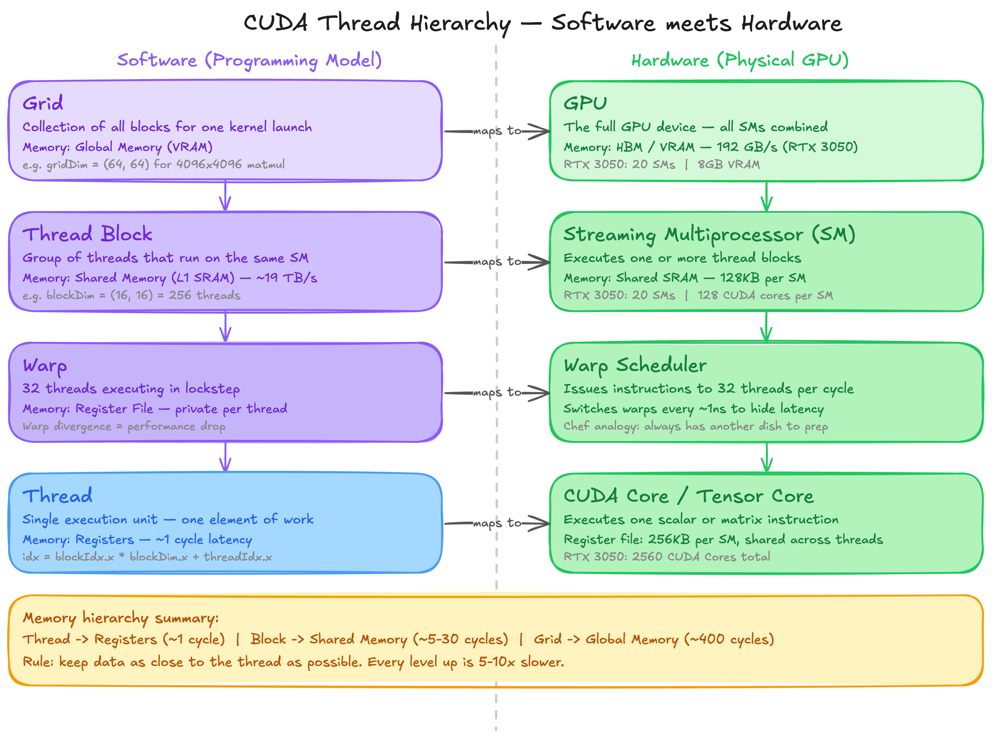
CUDA Thread Hierarchy — Software programming model maps to GPU hardware
A note on PTX and SASS
SASS is the assembly format for running programs on NVIDIA GPUs. It is the lowest-level format in which human readable code can be written and one of the formats output by NVCC alongside PTX. It is almost never manually written. Viewing compiler generated SASS and PTX while profiling and optimising high-level CUDA code is common practice. SASS is versioned and tied to a specific NVIDIA SM architecture.
PTX is both an instruction set architecture and an intermediate representation. It is forward compatible across GPU generations. The PTX components of a CUDA binary are compiled just-in-time at runtime. This is why different CUDA toolkit versions can target different GPU architectures without recompilation. It is also the source of the PTX compatibility error we hit earlier when the toolkit version exceeded what the driver supported.
CUDA Threads and Warps
A thread is the lowest unit of GPU programming. Each thread has its own registers and its own private program counter. This is what allows threads to independently track where they are in a program.
All threads in a warp share the same instruction pointer and execute instructions in lockstep. This design is intentional for performance. GPU threads also have stacks in global memory for storing spilled registers and function call frames. High performance kernels try hard to limit both of those things since global memory access is expensive.
A warp is a group of 32 threads. All threads in a warp are scheduled onto a single SM, and at minimum all warps from the same thread block land on the same SM. When threads in a warp diverge and need to execute different instructions, this is called warp divergence and performance drops sharply. The fraction of clock cycles in which a warp is issued an instruction is called the issue efficiency of the SM. Warps are a hardware feature that programmers do not directly control but must always be aware of.
One more concept worth knowing: the Warp Group. Introduced in NVIDIA Hopper architecture, a warp group is four contiguous warps used for large matrix multiplications. The warp rank of the first warp in a warp group must be a multiple of 4, where warp rank is simply the sequential index of a warp within its thread block.
CUDA Kernel
A CUDA kernel is similar to a function in CPU programming. The collection of threads executing a kernel is called a kernel grid, spread across the SMs of the GPU. In CUDA C++, kernels receive pointers to global memory on the device when invoked by the host CPU. The return type is always void since the kernel mutates memory directly rather than returning values.
This is why the host-device memory pattern looks the way it does:
// Host allocates device memory
cudaMalloc(&d_output, size);

// Kernel mutates it directly
kernel<<<grid, block>>>(d_output, d_input, N);

// Host reads the result back
cudaMemcpy(h_output, d_output, size, cudaMemcpyDeviceToHost);
The kernel never returns anything. It just writes to the memory address it was handed.
5. Thread Hierarchy in Practice — A 64x64 Matrix Example
Let’s make this concrete. Say we want to process every element of a 64x64 matrix. That is 4096 elements, each needing one thread.
We choose a block size of 16x16 — 256 threads per block. Our grid is then:
blockDim = (16, 16)    — 256 threads per block
gridDim  = (4, 4)      — 16 blocks total
Total threads = 16 x 256 = 4096
Each thread computes its unique row and column:
int row = blockIdx.y * blockDim.y + threadIdx.y;
int col = blockIdx.x * blockDim.x + threadIdx.x;
Each block owns a 16x16 tile of the output matrix. Thread (threadIdx.x=3, threadIdx.y=5) in Block(2,1) computes:
row = 1 * 16 + 5 = 21
col = 2 * 16 + 3 = 35
Responsible for element C[21][35]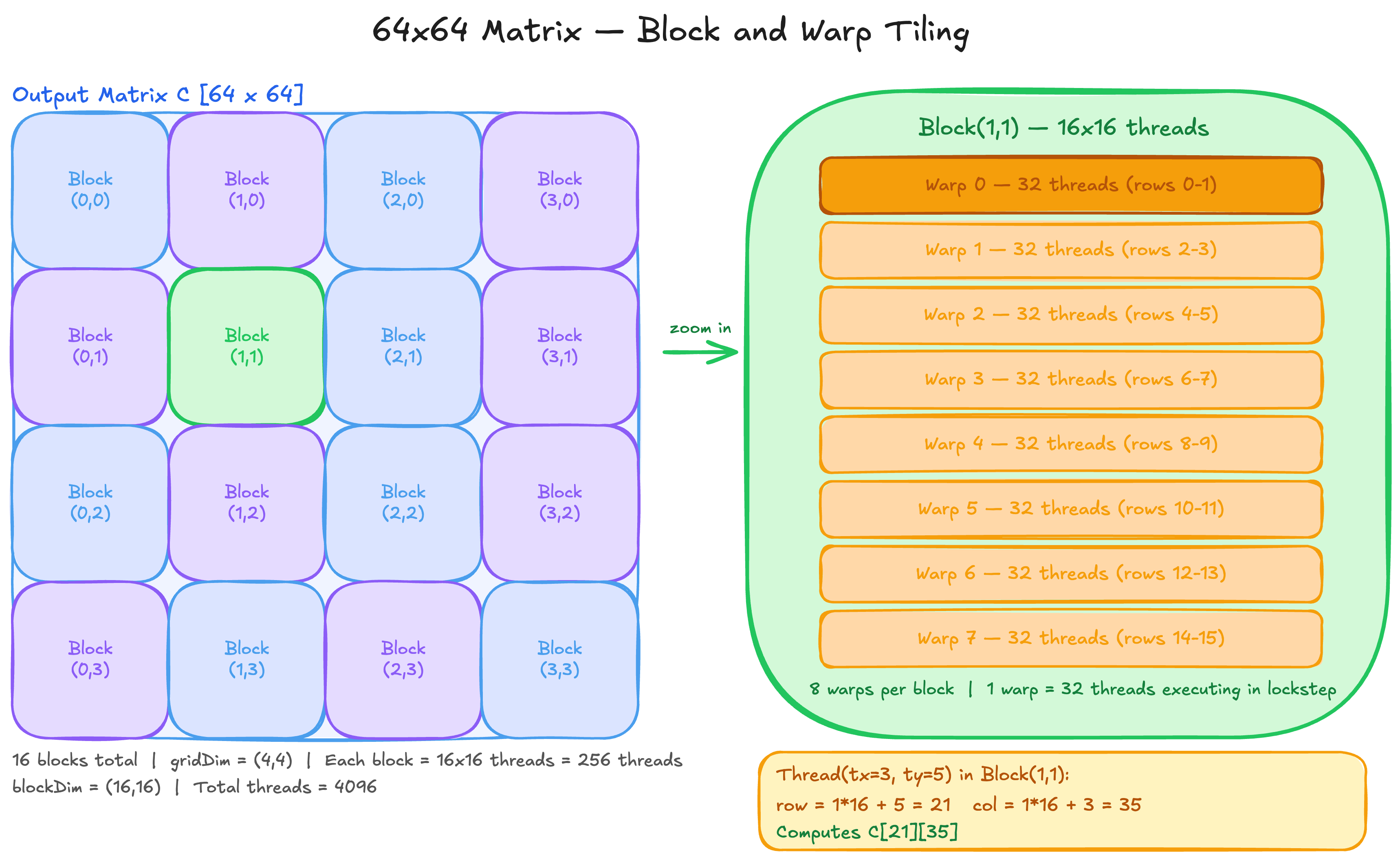
64x64 Matrix Tiling — 16 blocks, each block = 256 threads = 8 warps
Three Rules of Thread Coordination
Rule 1: Within a thread block — use __syncthreads() and shared memory
Threads within the same block can communicate through shared memory. But you must synchronise before reading what another thread wrote. This is exactly the pattern in tiled matmul:
As[threadIdx.y][threadIdx.x] = A[row * N + (m * TILE + threadIdx.x)];
Bs[threadIdx.y][threadIdx.x] = B[(m * TILE + threadIdx.y) * N + col];

__syncthreads();  // everyone must finish loading before anyone reads

for (int k = 0; k < TILE; k++)
    sum += As[threadIdx.y][k] * Bs[k][threadIdx.x];

__syncthreads();  // everyone must finish computing before next tile overwrites
Without the first __syncthreads(), thread A might read shared memory before thread B has finished writing to it. Silent wrong results, no crash.
Rule 2: Across blocks — use atomics on global memory
Blocks cannot use shared memory to communicate. Each block has its own shared memory invisible to others. The only shared space is global memory. If multiple blocks need to update the same location, you must use atomic operations:
atomicAdd(&global_sum[0], local_partial_sum);Atomics guarantee that read-modify-write happens as one indivisible operation. Without atomics, two blocks reading the same value and writing back will silently lose one of the updates. Atomics are expensive though. The standard pattern is to compute partial results within each block using shared memory, then use one atomic per block to combine into the global result.
Rule 3: Across blocks — assumed ordering is a race condition waiting to happen
There is no guaranteed execution order between blocks. Block 5 might finish before Block 0. If your algorithm requires Block B to see the results of Block A, split into two separate kernel launches:
kernel_A<<<grid, block>>>();
cudaDeviceSynchronize();   // wait for ALL of kernel_A to finish
kernel_B<<<grid, block>>>();
Any code that assumes Block B sees Block A’s writes without this synchronisation is a race condition. It may work in testing and fail in production when the scheduler orders blocks differently.
6. The Matrix Multiplication Problem
Now that we understand the hardware and the programming model, let us talk about the actual problem. Why is matrix multiplication interesting enough to dedicate an entire GPU to?
A matrix multiply C = A x B where A is M x K and B is K x N requires 2 x M x N x K floating point operations. For M = N = K = 4096, that is 2 x 4096^3 = 137 billion FLOPs. For a single forward pass of a large language model, this operation happens hundreds of times across all layers. The math is brutal.
The second reason matrix multiplication is interesting is that it exposes a fundamental tension: it is simultaneously compute intensive and memory intensive. How you balance these two determines your performance. This brings us to the roofline model.
7. The Roofline Model
Every GPU has two hard limits. A compute ceiling and a memory bandwidth ceiling.
Peak compute (RTX 3050):           9 TFLOPS
Peak memory bandwidth (RTX 3050):  192 GB/s
Ridge point:                       9000 / 192 = 46.9 FLOPs/byte
The ridge point is the crossover. If your kernel does less than 46.9 FLOPs per byte it transfers, you are memory bound. Adding more compute units will not help. If your kernel does more than 46.9 FLOPs per byte, you are compute bound. Adding more memory bandwidth will not help.
Arithmetic intensity is the metric that tells you where you sit:
Arithmetic Intensity = FLOPs performed / Bytes transferredAll three of our kernels sit deep in the memory bound region. Vector add is at 0.083 FLOPs/byte. Naive matmul is at 7.5 FLOPs/byte. Tiled matmul is at 11.2 FLOPs/byte. None of them are close to the ridge point of 46.9. Production kernels like cuBLAS sit at 50+ FLOPs/byte, right at or above the ridge point. That is the gap between what we wrote and what is used in production.
8. Three CUDA Kernels
I wrote three kernels from scratch on my RTX 3050 to understand all of this better. Here is what I built and what I found.
Kernel 1: Vector Add
The simplest possible GPU kernel. Two input arrays A and B, one output array C, where C[i] = A[i] + B[i]. Each thread handles exactly one element.
__global__ void vec_add_kernel(float* A, float* B, float* C, int N) {
    int idx = blockIdx.x * blockDim.x + threadIdx.x;
    if (idx < N)
        C[idx] = A[idx] + B[idx];
}
Launch:
int blockSize = 256;
int gridSize = (N + blockSize - 1) / blockSize;
vec_add_kernel<<<gridSize, blockSize>>>(A_d, B_d, C_d, N);
One thread, one element, one addition. Each thread gets a unique idx from its block and thread position, checks it is in bounds, and does its single addition. This is SPMD — Single Program Multiple Data. Same code, different data, executed by thousands of threads simultaneously.
Kernel 2: Naive Matrix Multiply
One thread per output element. Each thread independently computes the full dot product of one row of A with one column of B.
__global__ void mm_naive(float* A, float* B, float* C, int N) {
    int row = blockIdx.y * blockDim.y + threadIdx.y;
    int col = blockIdx.x * blockDim.x + threadIdx.x;
    if (row < N && col < N) {
        float sum = 0.0f;
        for (int k = 0; k < N; k++)
            sum += A[row * N + k] * B[k * N + col];
        C[row * N + col] = sum;
    }
}
The problem: each thread independently loads its entire row of A and column of B from global memory. For N=4096, every thread reads 4096 floats from A and 4096 floats from B. With 4096 x 4096 threads, each element of A gets read 4096 times from slow global memory. Massive redundancy.
Kernel 3: Tiled Matrix Multiply
A block of 16x16 threads cooperates to load a tile of A and a tile of B into shared memory, then computes partial dot products from fast on-chip memory.
#define TILE 16
__global__ void matmul_tiled(float* A, float* B, float* C, int N) {
    __shared__ float As[TILE][TILE];
    __shared__ float Bs[TILE][TILE];

    int row = blockIdx.y * TILE + threadIdx.y;
    int col = blockIdx.x * TILE + threadIdx.x;
    float sum = 0.0f;

    for (int m = 0; m < N / TILE; m++) {
        As[threadIdx.y][threadIdx.x] = A[row * N + (m * TILE + threadIdx.x)];
        Bs[threadIdx.y][threadIdx.x] = B[(m * TILE + threadIdx.y) * N + col];
        __syncthreads();

        for (int k = 0; k < TILE; k++)
            sum += As[threadIdx.y][k] * Bs[k][threadIdx.x];
        __syncthreads();
    }
    C[row * N + col] = sum;
}
Each of the 256 threads in a block loads one element of A and one element of B into shared memory. All 256 threads then reuse those same 512 values from fast shared memory instead of fetching from global memory again. Each value is reused 16 times instead of loaded 16 separate times.
9. Nsight Compute Results
I profiled all three kernels on my RTX 3050 with N=4096 using Nsight Systems and Nsight Compute. Here is what the analysis actually says.
| Metric | Vector Add | Naive Matmul | Tiled Matmul |
|---|---|---|---|
| Duration | 1.4 μs | 281.13 ms | 212.14 ms |
| Speedup vs Naive | — | 1x | 1.32x |
| Instructions | — | 9.4B | 6.7B (-28%) |
| Memory Throughput | — | 65.27 GB/s | 86.29 GB/s |
| DRAM Throughput | — | 30.02% | 39.69% |
| L1 Hit Rate | — | 87.14% | 0.02% |
| L2 Hit Rate | — | 48.65% | 47.01% |
| Shared Memory/Block | 0 KB | 0 KB | 2.05 KB |
| Shared Mem Loads | — | 0 | 3.22B |
| Achieved Occupancy | — | 99.90% | 99.90% |
| Warp Stall Rate | — | 73% | 74.45% |
The counter-intuitive finding
I expected tiled matmul to win because it saves memory bandwidth. Well, I was wrong.
Naive matmul has an 87% L1 hit rate. The hardware was already caching the row accesses automatically. The GPU’s L1 cache is smart enough to notice that 16 threads in the same warp are reading the same row of A and serve them all after the first miss. The bandwidth saving I was hoping tiling would provide was already happening for free.
So why is tiled matmul still faster? Instructions. Tiled executes 28% fewer instructions (6.7B vs 9.4B). Shared memory has deterministic single-cycle latency. L1 cache has variable latency. Over billions of instructions, that difference adds up to a 1.32x speedup.
The hardware was smarter than the theory I read. Tiling is still worth doing, just for a different reason than most explanations give.
What about the 0.02% L1 hit rate on tiled?
This confused me until I dug deeper. When you explicitly load data into shared memory, those loads bypass the L1 cache. The reuse is happening in shared memory instead. Physically, shared memory and L1 are the same SRAM on the SM. The difference is who manages it. L1 is hardware managed. Shared memory is programmer managed. Tiled matmul moved the reuse from hardware managed L1 to programmer managed shared memory. Same silicon, different controller.
10. Conclusion
We covered a lot of things in this blog. GPU hardware from SMs to HBM. The CUDA programming model from threads to grids. Matrix multiplication from naive to tiled. And Nsight Compute to see what is actually happening inside the GPU.
The key takeaway is not that tiled matmul is faster. It is that profiling told us WHY. Without Nsight, I would have assumed tiling saved memory bandwidth. With Nsight, I know it saves instructions. That distinction matters when you are trying to squeeze more performance out of a kernel.
The roofline model gives us the bigger picture. All three kernels are deeply memory bound, nowhere near the compute ceiling of the RTX 3050. The gap between what we wrote and what cuBLAS achieves is not a mystery. It is arithmetic intensity. Getting there requires deeper optimisations: register tiling, double buffering, warp-level matrix multiply instructions. That is where the real kernel engineering begins.Here is an interesting blog if you want to read about multiple matmul approaches on GPUs
The next question is obvious. We now understand how a GPU works and how to write kernels for it. But the systems that power LLM inference, vLLM, FlashAttention, speculative decoding, they go much further. How does vLLM manage GPU memory to serve thousands of concurrent requests? How does PagedAttention eliminate memory fragmentation? Why does KV cache matter so much?
That is exactly what the next post covers. We go deep into vLLM internals, PagedAttention, continuous batching and the memory management systems that make production LLM inference possible.
See you there.
Full code for all three kernels: github.com/kailashnagarajan/cuda-kernels